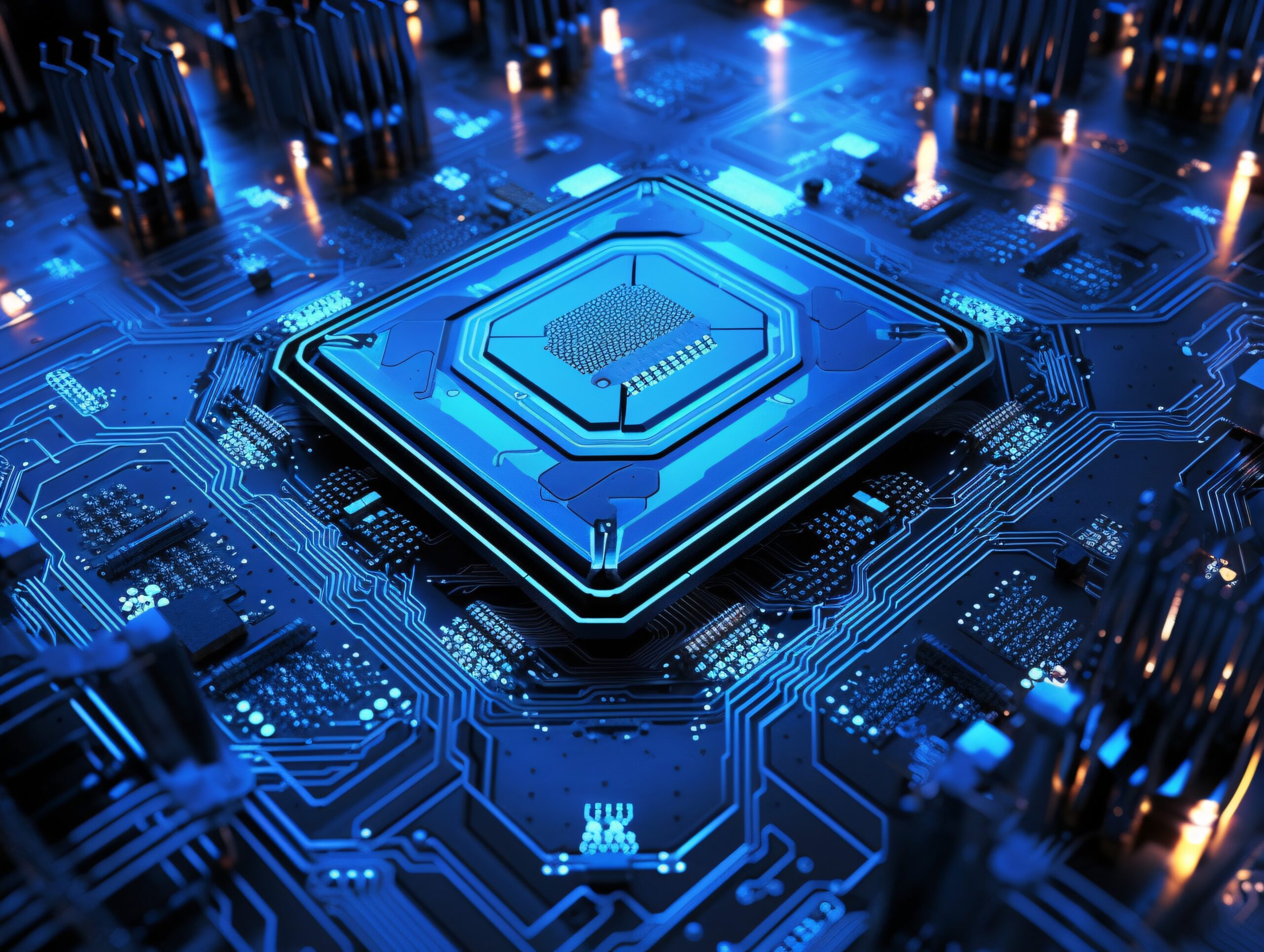
In the modern era of semiconductor manufacturing, where precision and miniaturization are key factors, the etching process plays a vital role. Etching is a sophisticated technique used to selectively remove layers of material from semiconductor wafers, enabling the creation of intricate circuit patterns. This article will delve into the art and science of the etching process in the semiconductor industry, exploring its techniques, applications, and other aspects.
Understanding the Etching Process:
In the semiconductor industry, Etching is the process used to remove layers or slices of a material, including metals, dielectrics, semiconductors and polymers. It can employ electrochemical electrolysis, chemical corrosion and even mechanical polishing arts. The two primary etching processes used in the industry are wet etching and dry etching.
Wet Etching:
Wet etching utilizes chemical solutions, known as etchants (liquid solution), to dissolve and remove specific materials. The etchant reacts with the exposed surface, removing the desired material selectively. This process requires careful control of etchant concentration, temperature, and immersion time to achieve the desired results. Wet etching is known for its simplicity, cost-effectiveness, and compatibility with a wide range of materials.
Dry Etching:
Dry etching, also known as plasma etching, employs a high-energy plasma to remove material from the wafers surface. The plasma consists of chemically reactive ions and radicals that bombard the wafer, breaking the molecular bonds of the material and causing it to be etched away. Dry etching techniques include reactive ion etching (RIE), plasma etching, and ion beam etching. Dry etching provides better control over the etching process, offers higher resolution, and enables the etching of more complex structures.
Applications of Etching Process in Semiconductor Manufacturing:
Etching plays a crucial role in various stages of semiconductor manufacturing, enabling the creation of intricate circuit patterns, interconnects, and semiconductor devices. Here are some key applications of etching in the industry:
- Integrated Circuit (IC) Fabrication: Etching is used to create patterns in the silicon wafer during the fabrication of ICs. It helps define features such as transistors, interconnects, and contact holes, allowing for the precise arrangement of components on the chip.
- Microelectromechanical Systems (MEMS): MEMS devices, such as sensors, actuators, and microstructures, rely on etching techniques to define their intricate structures. Etching enables the production of microscale components with high precision and repeatability.
- Semiconductor Packaging: Etching is employed in the packaging stage of semiconductor manufacturing to create cavities and trenches for interconnects and wire bonding. It ensures proper electrical connections and protects the delicate components within the package.

Conclusion
Well, the semiconductor industry is an ever-evolving industry characterized by rapid evolution, encompassing a multitude of dynamic manufacturing processes. So, if you are interested in knowing about this industry in depth, or are willing to make a career in the VLSI industry, Chipedge is the right place for you. It is one of the best training and placement institutes in Bangalore that offers several VLSI courses including job-oriented courses in Bangalore and VLSI Physical Design Course for both freshers as well as professionals. Contact us to know more.