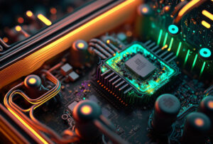
The relentless demand for electronic devices in today’s world underscores the critical role of the VLSI industry in shaping modern technology. With its ability to create intricate integrated circuits, the VLSI course has paved the way for smaller, faster, and more efficient devices. For those aspiring to thrive in this dynamic field, a deep understanding of physical design is indispensable. Chipedge, the best VLSI training institute in Bangalore, offers a comprehensive course covering Design Verification, Physical Design, and DFT, ensuring students are well-prepared for success in the industry. In this article, we delve into some fundamental Physical Design interview questions to aid you in excelling on your VLSI career path.
Q1. What are the types of checks done in physical design interview questions?
- LVS (layout vs schematic) – Ensures the physical layout accurately reflects the circuit schematic.
- DRC (design rule check) – Verifies the layout adheres to the foundry’s manufacturing guidelines.
- ERC (electrical rule check) – Analyzes potential electrical issues like shorts, opens, and excessive current densities.
- LEC (logical equivalence check) – An advanced check for highly optimized designs, it compares the functionality of the layout to the golden RTL.
Q2. How to fix setup and hold violations at a time?
It’s generally not possible to address both simultaneously because reducing data path delays improves hold but worsens setup timing. Here are approaches for each violation:
Setup:
- Reduce buffers in the path (each adds delay).
- Substitute buffers with inverter pairs (introduce less delay).
- Replace high-voltage threshold (HVT) cells with low-voltage threshold (LVT) cells (LVTs are faster).
- Increase buffer/driver size (lowers output resistance and reduces delay).
- Insert repeaters (additional buffering stages).
- Adjust cell placement strategically.
Hold:
- Increase delays in the data path (opposite of setup fixes).
- Decrease buffer/driver size (increases output resistance and delays signals).
Q3. How can you avoid cross-talk?
Cross-talk is the undesirable electrical influence between adjacent nets. Here are techniques to mitigate it:
Spacing: Increase the distance between the aggressor (noise-coupling net) and victim (noise-receiving net).
Shielding: Insert grounded metal layers between nets to absorb noise.
Stable supply: Maintain a clean and stable power supply to reduce ground bounce.
Cell sizing: Upsize victim cells to improve noise immunity.
Layer jumping: Route on different metal layers to increase separation between nets.
Victim net width increase: Reduce victim net resistance to make it less susceptible to noise.
Guard rings: Surround sensitive circuits with grounded metal rings to shield them from noise.
Q4. What is cross-talk?
Cross-talk is the unwanted capacitive coupling between nets that causes electrical interference. When two nets run close together, a switching signal on one can induce a small current in the other, potentially causing errors.
Q5. What is scan chain reordering?
Scan chain reordering optimizes the routing of scan chains used in testing by rearranging their connection order. This improves timing closure and reduces congestion during place and route (P&R).
Q6. What is the concept of rows in the floor plan?
In the floor plan, standard cells are placed in rows of equal height and spacing, with variable width. Each row connects to power and ground rails (VDD and VSS) for power delivery. In some technologies, rows can be flipped to share power rails in a VDD-VSS-VDD pattern.
Q7. What are the advantages of NDRs (Non-Default Rules)?
NDRs are special placement rules that offer benefits such as:
Reduced electromigration (EM) risk: By applying double-width routing, NDRs help prevent EM, a reliability concern where metal atoms move due to high current density.
Mitigated cross-talk: Double spacing between nets using NDRs reduces cross-talk by increasing the physical separation.
Alleviated congestion: NDRs can ease congestion issues in lower metal layers by providing more routing space.
Enhanced pin accessibility: Strategic NDR placement can improve the accessibility of standard cell pins for easier routing.
Q8. What is temperature inversion?
Temperature inversion refers to the phenomenon where cell delay in CMOS circuits behaves differently depending on the technology node.
Higher technologies (above 65nm): Cell delay typically increases with rising temperature due to increased carrier scattering.
Lower technologies (below 65nm): Cell delay can become inversely proportional to temperature. This is because leakage currents increase significantly at higher temperatures, reducing the effective gate oxide capacitance and leading to faster switching.
Q9. In a register-to-register path with a setup problem, where would you insert a buffer?
To fix a setup violation in a register-to-register path, a buffer can be inserted near the launch flip-flop. This reduces the transition time on the data path, minimizing wire delay and consequently improving arrival
Conclusion
Mastering VLSI Physical Design is paramount for success in the semiconductor industry. Chipedge’s comprehensive VLSI course equips students with the requisite skills and knowledge to excel in their careers. By familiarizing yourself with key physical design concepts and addressing interview questions effectively, you can embark on a fulfilling journey in the VLSI domain, shaping the future of technology. If you are interested in learning more about VLSI design methodologies contact ChipEdge, offering the best VLSI design course in Bangalore.