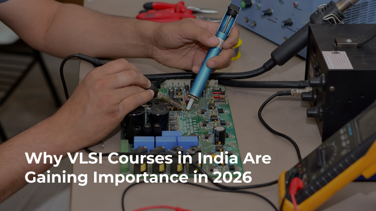
The semiconductor industry in India is booming. Revenues are expected to reach USD 400 billion by 2026, driven by a rapidly growing consumption market. To ride this wave of growth, you need the right skills and the right time to acquire them is now. The India Semiconductor Mission has sanctioned funding to multiple entities to support the upskilling of professionals in the domestic semiconductor industry. Major global semiconductor companies have set up design centers in India which shows the demand for skilled VLSI design course professionals in recent times.
The Indian government’s Make in India initiative is focusing on transforming India into a manufacturing hub for the entire world. This will create a need for electronics education and engineering design professionals creating an increase in VLSI production for all corners of the globe. The importance of new and optimized electronic equipment in the defense and automotive industry is another factor pushing the growth of VLSI design course professionals in India. Last but not least, the Indian indigenous satellite program has risen to unprecedented heights in recent years and the future promises to deliver countless opportunities for cutting edge engineering in the electronics field.
Why VLSI Certification Matters in 2026
The semiconductor industry is growing exponentially, and we are surrounded by products that use chips in our daily routines. Unfortunately, India does not have enough expertise to meet the industry’s requirements for chip design, verification, and physical design implementation. The semiconductor talent gap in India has widened significantly, and the industry predicts that over 300,000 positions will go unfilled by 2025.
Chip design companies in India need a constant stream of graduates who bring industry-standard electronic design automation (EDA) tool proficiency and the right skillsets for the specific job roles. These factors make Cadence / Synopsys / Mentor Graphics physical design training or VLSI Design Verification Training from professional EDA tool consultants mandatory for your entry into any chip design company. Companies are not only looking for the best but are also hiring only the ‘already-trained-best’. Hence, a VLSI certification course from professional EDA tool consultants becomes a necessity.
Top VLSI Training Options Across India
What makes certain VLSI institutes stand out among the sea of options? It’s all in the curriculum! The more they delve deep, from fundamentals to current industry standards, the easier it is for you to make your choice. Being the melting pot of all modern silicon technologies, VLSI training demands strong industry relationships.
Look for partners and tie-ups with expert hardware developers and industry bodies. This helps monitor evolving trends and statistics. Last but definitely not least – perhaps you are taking this course to get a job, after all – is their placement history. Most top Virtual Labs do not simply ‘hire’, they absorb. So if you want to enter the world of VLSI/ASIC, get ready for some serious, fun, hands-on learning!
Specialized Course Tracks Worth Considering
While analog design as a subset is included in the VLSI/ASIC curriculum, the essential differences are obvious. This area demands a higher order of abstraction, according to business needs and application requirements. Hence, specialized training comprises a much deeper understanding of transistor-level designing, noise margins, and mismatch analysis.
Moreover, tape-outs involve numerous iterations before the design is set in silicon. Hence, the utmost familiarity of automated tool environments, especially for layout design, is essential. This makes you productive in the shortest time. You can even adapt to alternate design systems or customize tools for specific requirements. Are such things covered in conventional training? A big doubtful nod is the answer!
Making Your Choice in 2026
How do you decide which VLSI program is the right fit for you? It’s a personal choice that depends on a few different factors. Your career goals, your budget, whether or not you can commit to an in-person program, the amount of time you can dedicate, your learning preferences, etc., these aspects should all be taken into account before making a decision. Are you looking for an extensive VLSI training in India? Read on to see the different types of programs available to you. Then, once you’ve looked at your options, don’t forget to choose an institute with the best vlsi design course in India. Look for those that offer updated course content regularly.
Once you find that, the next step will be making your decision for which institute in India to go to. If, after completing the VLSI training, your goal is to be among the highly paid VLSI design engineers, then continue reading to understand what you need to do to get there. However, if you are having second thoughts about the industry and its growth potential, then no amount of training will be fruitful. Given the expected growth of the semiconductor industry in the next few years, the demand for VLSI design engineers is on the rise. So let’s get into the necessary details that you need to know before making an educated decision.


