


Online
Design for Test
- Weekend Batch Sat-Sun
- 6 Months Duration
Learn the Design For Test, the in-demand skill and highly paid job in Semiconductor Industry. Learn from ChipEdge, which has the proven track record for last 13+ years
VLSI professionals can build a rewarding and challenging career with DFT Online Courseand DFT Training. Design For Testability, commonly called as DFT is a specialization in the SOC design cycle, which facilitates design for detecting manufacturing defects.
Unlike functional verification, which ensures that the design works as intended, the DFT course deals with verifying the test structures added to make the design testable after fabrication.
Everything you need to go from learner to professional in one powerful program.
Learn from experts in Design For Testing
Practice on industry-grade EDA Tools
Access curated reading material, PDF, notes through our LMS
Earn ChipEdge Certification recognized by industry
Group sessions with mock interviews and soft skills session for resume building and job hunting.
Get exposure on industry grade projects, by solving complex problems.
Choose from weekend, weekday, or self-paced tracks that fit your schedule.
Dedicated placement cell with mock interviews, job referrals, and 200+ hiring companies.
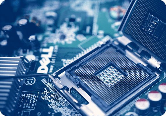
Design For Test (DFT) is a specialized domain in VLSI that incorporates testability features into an integrated circuit during the design phase. It ensures that manufactured chips can be efficiently tested for defects, improving product quality, reliability, and yield.
DFT engineers work with scan insertion, ATPG, boundary scan, memory BIST, compression techniques, and fault analysis to enable effective post-manufacturing testing. As chip complexity continues to increase, DFT has become an essential function across semiconductor companies developing processors, automotive electronics, networking devices, and advanced SoCs.
Essential Test Engineering Domain in Modern VLSI
Master Scan, ATPG, MBIST & Industry Test Flows with our Industry-Aligned curriculum
Average Salary Range for Entry-Level DFT Engineers in India
Leading Semiconductor Companies Recruiting DFT Engineers
Six compelling reasons why this is the best investment you'll make in your career.
Build YourVLSI Career with confidence, learn from ChipEdge, a leader with proven track record of 13+ years of expertise.
Explore a career path for global career opportunities. Design For Test professionals are in-demand across leading semiconductor companies.
Gain hands-onexperience with industry standard Synopsys tools like BSD Compiler, SD Compiler, TetraMax, VCS widely used in top semiconductor companies.
Work on practical industry-style projects where you perform scan insertion, ATPG generation, fault coverage analysis, scan compression implementation, and DFT validation on complex digital designs following semiconductor industry workflows.
Get resume-building assistance, mock interview preparation, aptitude guidance, and placement support through hiring partnerships and industry connections.
Build expertise that opens opportunities in advanced domains such as Scan Architecture, ATPG and Fault Diagnosis, Memory BIST (MBIST), Logic BIST (LBIST), Test Compression Techniques, Automotive Functional Safety Testing, and Advanced SoC Test Solutions.
Choose the format that fits your schedule and learning style.
Best for freshers & students who prefer classroom-based training with direct trainer interaction.
Includes:
Best for working professionals and learners (freshers, students) who prefer online learning without relocating.
Includes:
Best for learners who want flexibility and structured content for their learning at their own pace.
Includes:
Choose the batch that works best for your schedule. Limited seats available.
Industry Standard Synopsys tools you'll master and add to your professional portfolio.
This course is designed for anyone ready to break into tech or level up their career.
B.Tech / M.tech Students who is pursuing pre-final/final year and want to pursue a VLSI Career in Design For Test
B.E / B.Tech / M.E / M.Tech graduates from ECE,EEE, Telecom, CSE, and related branches looking to start a career in VLSI.
Professionals aiming to transition into VLSI Design For Test or upgrade their skills with hands-on industry-oriented training.
Get enrolled in 4 easy steps — the whole process takes less than 30 minutes.
Complete our quick online form with your basic details and preferred learning mode.
Our Learning Advisor will call within 30 minutes to discuss your goals and recommend the best batch.
Pay the registration fee online. Choose from full payment, installments, or education loan options.
Get access to LMS, join your batch's community, and begin your journey on day one!
Industry focused VLSI Training Programs designed to transform fresh graduates into semiconductor professionals.
Courses designed by industry experts with 25+ yrs of industry experience.
Dedicated placement support by arranging interview opportunities with leading VLSI Companies
Access cloud-based VLSI lab infrastructure and practice Design For Test anytime from anywhere.
Gain hands-on experience with industry-standard Synopsys EDA tools including BSD Compiler, SD Compiler, TetraMax, VCS.
Prepare for real VLSI interviews with technical mock sessions, HR rounds, and resume-building guidance.
ChipEdge offers flexible payment options to help learners begin their VLSI journey without financial pressure.
Affordable monthly installments to spread your investment over time
No additional fees on selected payment plans
No Cost EMI as per eligibility
Take the first step towards a high-paying tech career. Our learning advisors will guide you through every step.

Talk to our expert & choose the right course for you
🔒 No spam. 100% Free. Our expert will call within 24 hrs.
Our Placement Desk works closely with leading VLSI companies to support their hiring needs for entry-level skilled engineers. We arrange interview opportunities with both multinational semiconductor companies and service-based organizations.
Placement support is provided as a complimentary service until the candidate secures a job opportunity. Registered candidates receive dedicated guidance including resume Preparation, interview scheduling, mock interviews, and career mentoring.
Hiring Companies
Learners Trained Across VLSI Domains
Group Mock Interviews, Resume Building & Interview Preparation
Placement Support Until You Get Placed


The VLSI Design For Test (DFT) Course is designed to prepare aspiring engineers for specialized careers in semiconductor testing and VLSI design. The curriculum aligns with current industry practices and test methodologies used by top semiconductor companies.
With practical exposure to industry-leading tools including BSD Compiler, SD Compiler, TetraMAX, and VCS, learners develop hands-on skills in scan architecture, automatic test pattern generation (ATPG), fault diagnosis, test compression, and DFT validation. This comprehensive training enables learners to work confidently on complex ASIC and SoC designs across modern semiconductor applications.
Real stories from real people who transformed their careers with ChipEdge.

I have completed my DFT course from ChipEdge. Trainers are very good and informative. Materials and recorded sessions can be accessed in LMS portal which is very helpful. The lab access through VPN has helped me to have good hands on training. The topics explained by the instructor is very clear, where sir had good patience level to explain the topics. Trainers address the problems individually. Training was helpful for placements. Thank you ChipEdge.

I pursued DFT course from ChipEdge, the instructor was excellent, the best I've experienced, and I couldn't imagine him doing a better job of seamlessly walking students through a breadth of information. He did a fabulous job pacing everything and addressing student questions. There were no problems with connectivity. Just wanted to let you know that the service provided, from registration to training was a very positive experience for me. I intend on taking more courses in the future and referring friends/family members to take courses at ChipEdge. Thank you ChipEdge.

I have completed my DFT course from ChipEdge. Trainers are very good and supportive, he has very good patience. The topics explained by the instructor is very informative and useful. The Training was helpful for placements. Lab and LMS access are very good. Recently I got selected in Tesolve through chipEdge. The process in ChipEdge is easy going in every step. They always coordinate with us. I would like to thank each and every one in ChipEdge who helped me from initial admission till placement. Thank you ChipEdge.
Everything you need to know before enrolling.
Design for Testability (DFT) is a methodology used to make integrated circuits easier to test for manufacturing defects after fabrication. Techniques such as scan insertion and BIST help improve fault detection and chip quality. A VLSI Design for Testability (DFT) Course helps engineers understand these concepts and learn DFT from Scratch with practical industry applications.
DFT enables efficient testing of manufactured chips, helping identify defects before products reach the market. It improves fault coverage, product reliability, and manufacturing yield. A VLSI DFT Course teaches how DFT contributes to the successful development of ASICs and SoCs.
ATPG (Automatic Test Pattern Generation) creates test vectors that detect faults such as stuck-at and transition faults in a circuit. It plays a key role in improving fault coverage and test quality. These concepts are covered in an ASIC DFT Course through practical testing workflows.
A scan chain connects flip-flops into a shift-register structure, allowing engineers to control and observe internal circuit states during testing. Scan chains are essential for detecting manufacturing defects and are a core topic in DFT Engineer Training.
Popular DFT tools include Synopsys DFT Compiler, Tetramax, Siemens Tessent, and Cadence Modus. These tools are used for scan insertion, ATPG, and fault analysis. Hands-on exposure to these tools is commonly included in a VLSI Design for Test Course.
Built-In Self-Test (BIST) allows a chip to test itself using embedded test logic. Common types include Logic BIST (LBIST) and Memory BIST (MBIST). These techniques are important topics in Chip Testing Courses and in modern semiconductor testing flows.
Yes, DFT is a highly specialised and in-demand field within the semiconductor industry. Engineers with DFT skills are sought after by ASIC design companies and semiconductor manufacturers. Completing a VLSI DFT Course with Placement from a reputed Design for Test Institute can improve career opportunities.
Freshers with relevant DFT skills typically earn between ₹4–16 LPA, while experienced engineers can earn more based on their experience. A structured online DFT training program or an online DFT Course for Freshers can help build the skills required for these roles.
Functional testing verifies whether a chip performs its intended operation, while scan testing focuses on detecting manufacturing defects through scan chains. Both approaches are important in semiconductor development and are covered in a VLSI Testing Course and a VLSI Backend Testing Course.
Get the latest VLSI news, updates, technical resources
© ChipEdge. All Rights Reserved.


