People usually imagine chip design as engineers sitting and writing Verilog all day. That’s part of it, but not the full picture.
In reality, VLSI design is a long process where every stage affects the next one. Something as small as an RTL coding mistake can eventually create timing failures during backend implementation. Sometimes the issue doesn’t even show up until much later in the flow.
That’s why engineers spend so much time understanding the complete design process instead of focusing only on coding.
It Always Starts with Requirements
Before anyone writes RTL, teams first decide what the chip is supposed to do.
How fast should it run?
How much power can it consume?
What interfaces are needed?
How large can the design become?
These early decisions shape almost everything later. A weak architecture usually creates problems throughout the project.
Good planning saves a surprising amount of debugging time.
RTL Coding Is Only One Part
Once the architecture becomes clear, engineers begin writing RTL using Verilog or VHDL.
This stage looks simple from outside. But writing RTL that works reliably is harder than most beginners expect.
A module may simulate correctly and still fail later because of timing issues, reset handling, or integration behavior. Small oversights become difficult to trace once designs grow larger.
That’s why experienced engineers care a lot about clean and readable RTL.
Verification Usually Takes More Time
Many freshers assume coding is the biggest task. In actual projects, verification often consumes more effort.
Teams build testbenches, run simulations, debug waveforms, and test corner cases repeatedly. The goal is simple: catch problems before fabrication.
Because once silicon is manufactured, fixing bugs becomes extremely expensive.
Sometimes engineers spend hours debugging a failure caused by one missed condition in a state machine.
That’s normal in VLSI projects.
Synthesis Changes the Design into Gates
After verification, the RTL moves into synthesis.
Here, tools convert the design into gate-level logic while trying to meet timing, area, and power targets. Reports become important during this stage because they reveal critical paths and possible violations.
Students usually find synthesis interesting because this is where the design starts feeling more “real.”
You begin seeing how coding style affects hardware implementation directly.
Backend Design Brings Physical Challenges
Then comes physical design.
Placement, routing, clock tree synthesis, congestion analysis, timing closure — this is where physical limitations start affecting the design heavily.
A design that worked perfectly in simulation can suddenly struggle because routing delays increase timing paths.
This surprises many beginners.
Frontend and backend are far more connected than they first appear.
DFT Is Important Too
Testing manufactured chips is another major part of the process.
Design for Testability, usually called DFT, helps engineers identify faults after fabrication. Scan chains and built-in self-test structures make testing practical for complex chips.
Without DFT support, production testing becomes much harder and more expensive.
Tape-Out Is the Final Milestone
Once verification, timing analysis, synthesis, and physical checks are completed, the design reaches tape-out.
This is the stage where the final layout gets prepared for fabrication.
By this point, teams want extremely high confidence because mistakes after tape-out are costly and difficult to fix.
For many engineers, tape-out day feels like the end of a marathon.
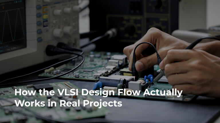
Why Hands-On Practice Matters So Much
VLSI cannot really be learned through theory alone.
Reading about synthesis or STA is one thing. Debugging an actual timing violation is completely different.
Students improve much faster when they work with tools directly and build small projects themselves. FPGA implementation, waveform debugging, timing analysis — these experiences develop real understanding.
That’s usually when the design flow stops feeling confusing.
Common Tools Used in VLSI
Most semiconductor workflows rely on industry-standard EDA tools such as:
- Synopsys Design Compiler
- PrimeTime
- Cadence Innovus
- Mentor Questa
At first, the reports and logs may look overwhelming. Over time, though, engineers start understanding what the tools are actually showing.
And that confidence matters a lot during interviews and real projects.
Career Paths After Learning VLSI
Students familiar with the VLSI flow can move into different semiconductor roles:
- RTL Design Engineer
- ASIC Verification Engineer
- FPGA Engineer
- Physical Design Engineer
- DFT Engineer
Most freshers begin with smaller module-level work before handling larger chip integration tasks.
FAQs
What is the VLSI design flow?
It’s the complete process used to design and implement a chip from specifications to fabrication.
Is VLSI difficult for beginners?
Initially yes, mainly because multiple stages are connected. Practical learning makes the process easier to understand.
Why is verification important?
Verification helps identify functional issues before manufacturing, where fixes become expensive.
Which tools are commonly used in VLSI?
Synopsys Design Compiler, PrimeTime, Cadence Innovus, and Mentor Questa are widely used in semiconductor workflows.
Does VLSI include physical design?
Yes. Placement, routing, timing closure, and floorplanning are all part of the overall design flow.
What jobs can students apply for after learning VLSI?
Students commonly pursue RTL, verification, FPGA, physical design, and DFT roles.


