
Building Confidence While Learning VLSI Concepts
Importance of Confidence in Technical Learning Very Large Scale Integration (VLSI) is intimidating. It deals with microscopic structures. It involves […]
Importance of Confidence in Technical Learning Very Large Scale Integration (VLSI) is intimidating. It deals with microscopic structures. It involves […]
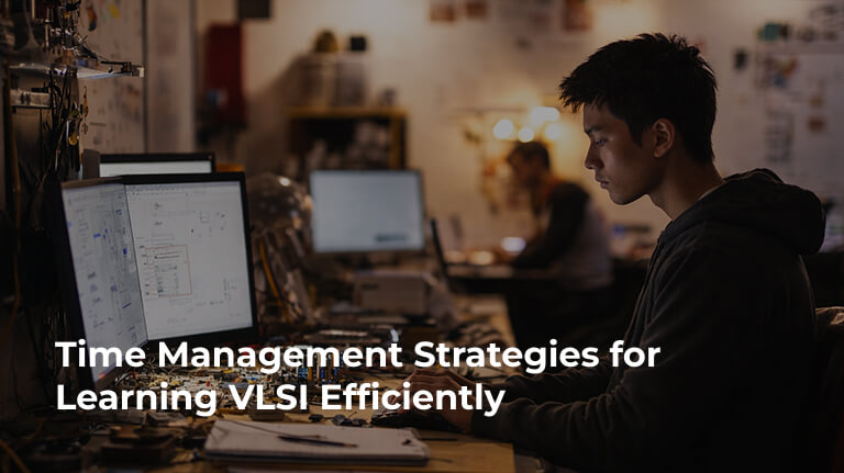
Importance of Time Management in Learning Very Large Scale Integration (VLSI) is a vast field. It covers digital logic, verification,
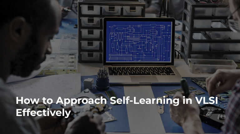
Introduction to Self-Learning Very Large Scale Integration (VLSI) is a complex field. It involves designing chips with millions of transistors.
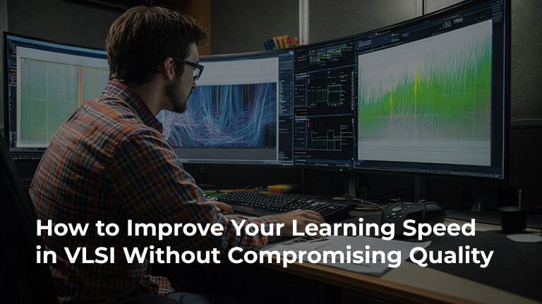
Understanding Learning Speed in Technical Fields Very Large Scale Integration (VLSI) is dense. It combines physics, logic, and software. Many
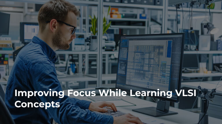
Importance of Focus in Technical Learning Very Large Scale Integration (VLSI) is not a subject you can skim. It requires

Introduction to Consistency in Learning Very Large Scale Integration (VLSI) is not a sprint. It is a marathon. The field

Introduction to Skill Gaps in Technical Learning Learning Very Large Scale Integration (VLSI) is not a straight line. It is
Introduction to Industry Expectations The semiconductor industry is not like a university classroom. In school, you solve problems with clear
Introduction to Common Challenges Very Large Scale Integration (VLSI) is a demanding field. It combines physics, logic, and software engineering.
Introduction to Learning Mistakes Very Large Scale Integration (VLSI) is hard. It is not just about knowing logic gates. It
Get the latest VLSI news, updates, technical resources


282 (4th & 5th Floor), 7th Main Rd, stage2, BTM Layout, Bengaluru, Karnataka 560076
© ChipEdge. All Rights Reserved.

