Graduating with an ECE degree means you have a wealth of knowledge—logic design, microprocessors, VLSI fundamentals—but entering the workforce can feel overwhelming. Employers seek hands-on experience with tools that were never part of your curriculum. Job postings demand projects that classroom labs simply can’t provide. It’s disheartening to feel equipped on paper but unprepared for real-world applications.
This is where many graduates find themselves at a standstill. The disparity between academic teachings and industry requirements can be significant. Employers are looking for candidates who can immediately engage with EDA tools. Meanwhile, graduates often struggle to find effective training that goes beyond theoretical concepts.
That’s why ChipEdge was established—to close that gap. We prioritize practical, industry-focused training.Our VLSI courses are designed to transition students from theory to hands-on practice. If you’re on the hunt for the top courses tailored for ECE students, your search ends here.
 Explore Our Programs
 Get in Touch
Why Our Program Stands Out forVLSI Enthusiasts


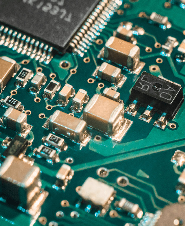
Many training programs attempt to condense intricate chip design into a handful of lectures. However, mastering this fieldFPGA Designis akin to learning to swim—you can’t become proficient just by reading about it. You need to dive in.
Our courses are crafted with this principle at heart. Rather than just providing slides and notes, our programs:
- Replicate the actual flows used by semiconductor firms.
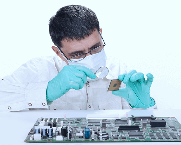
- Offer hands-on access to real tools, enabling practice on genuine designs.
- Include interactive sessions with trainers who have extensive industry experience.
- Incorporate projects into the curriculum to give students an edge in job interviews.
This isn’t generic skill enhancement. It’s focused learning, tailored to align with industry practices. That’s what distinguishes these programs as some of the best courses for ECE students in India.
Every student has unique interests and strengths. Some enjoy working with circuits and layouts, while others excel at debugging. Some aim to specialize in niche areas. We have organized our programs into three main learning tracks that correspond to actual job roles in chip companies. This track emphasizes taking a design from RTL to layout and signoff. If you enjoy working on the physical aspects of a chip and understanding its layered construction, this is where you’ll excel. What you’ll learn:
Why this program is essential:
FPGA Design specialistsare essential for chip tapeouts. By completing this course, you’ll navigate the same processes used in leading semiconductor companies. Verification ensures that the design functions as intended. This role is in high demand across the industry, as errors in silicon can be extremely costly.
What you’ll gain:
Why this program is vital:
Companies seek verification engineers who can quickly adapt and start developing verification environments. You’ll gain enough practical experience to confidently discuss your skills in interviews and, more importantly, to contribute effectively from day one. DFT focuses on ensuring a chip is testable post-manufacturing. It’s a specialized area with fewer candidates and an increasing number of job openings.
What you’ll gain:
Why this program is essential:
DFT specialists are sought after as companies value engineers who can lower testing costs and enhance yield. Adding this expertise can make your profile shine in a competitive job market. Key Learning Tracks You CanSelect From


Choosing theBest Learning Journey
There’s no single path for everyone. Some learners start with verification and later explore physical design, while others dive into physical design first due to their passion for circuits. The important part is to tailor your learning to your interests.
Here’s a straightforwardmethod to choose:
- If you’re passionate about how circuits evolve into actual chips — working on layouts and preparing designs for production — begin with Physical Design (PD).
- If you enjoy debugging, testbenches, and logic, focus on Verification.
- If you’re intrigued by how chips are evaluated for manufacturability before fabrication and want to acquire a highly sought-after skill, opt for Design for Test (DFT).
- If you aspire to have a diverse skillset, merge two tracks — for instance, DV and DFT.
Numerous students atChipEdgedo just that: they establish a solid foundation with one course and then add a second. This approach creates a profile that attracts recruiters.
Typical Learning Pathfor aspiring engineers
- Update your digital skills andFPGA fundamentals.
- Select your primary track.
- Engage in hands-on tool sessions and organized labs.
- Develop your capstone project.
- Prepare for interviews with practice sessions and portfolio evaluations.
- Receive placement assistance from ChipEdge’s partner network.
By adhering to this framework, you’re not merely learning — you’re charting a clear path to employment. This is what makes these courses ideal for ECE students aiming for careers in core VLSI.
Beyond the Basics:What Sets ChipEdge Apart
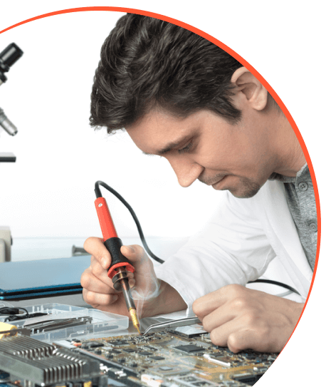

Hands-On Tool Experience:You gain access to Synopsys licenses and VPN connections to labs, allowing you to practice from anywhere.

Career Guidance:You’ll get support with resume crafting, mock interviews, and introductions to potential employers.

Adaptive Learning:Weekend classes make it convenient to learn alongside your college or job.

Project-Based Approach:You’ll undertake real chip design projects, not just view presentations.
This ecosystem enables students to transition from theoretical knowledge to job-ready abilities. Instead of learning in isolation, you collaborate in a manner similar to professionals in design firms.
 Join Us Today
Why VLSI StudentsChoose ChipEdge
The courses are tailored to meet actual hiring demands. Rather than concentrating solely on what’s ‘nice to know,’ they focus on what employers truly seek during interviews and require on the job. This is why many graduates fromVLSI backgroundssecure their initial positions in physical design, verification, or DFT shortly after finishing the program.
And since the tools and processes reflect real industry environments, the learning curve upon placement is significantly reduced. You arrive already familiar with workflows, terminology, concepts, and debugging techniques.
For students who have spent years grasping theory in classrooms, this can be a pivotal moment — transitioning from merely understanding concepts to actually creating functional designs.
Key Takeaways
Selecting the ideal courses for ECE students goes beyond merely finding a training program — it’s about discovering a pathway between your current position and where the industry expects you to be. ChipEdge’s learning environment is structured to make that pathway tangible.
If your aim is to enter the field ofFPGA Development, verification, or test engineering, this is an excellent starting point — equipped with tools, mentors, and a framework that truly works.

Inquire NowToday
FAQs
If debugging and logic inspire you, begin with Design Verification. If circuits and layouts captivate you, choose Physical Design. Those who want to excel often blend two tracks for a more robust profile.
Absolutely. Many students start while completing their college education. Pre-course refresher modules are available to help you catch up swiftly.
Indeed. ChipEdge offers Synopsys tool licenses and VPN access to labs, allowing you to gain practical experience like a semiconductor engineer.
Definitely. Our placement team provides resume assistance, conducts mock interviews, and connects you with potential employers. We support you until you land a job.
Yes, many students choose this path. For instance, combining DV and DFT is a popular strategy that enhances job prospects in both design and testing.
Subscribe to Our Updates
Stay updated with the latest in VLSI, news, and technical resources.


Privacy Policy| ©2026ChipEdge. All Rights Reserved.