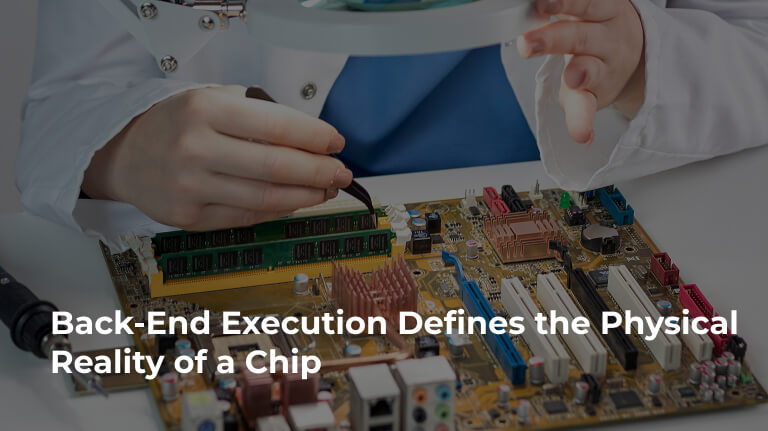
Transition from Design to Layout
Front-end design ends with a netlist. Back-end execution begins with that netlist. This transition matters. You move from abstract logic to physical geometry. Wires become metal layers. Gates become transistor layouts. Timing constraints become placement rules. The shift is not automatic. You must translate intent into geometry. If you are exploring a vlsi physical design course, you will see how this phase turns code into silicon. Chipedge emphasizes this practical transition in their training modules. You learn to read floorplan reports. You learn to interpret placement density maps. You learn to debug routing congestion. These skills separate designers from implementers.
Organizing Floorplans Efficiently
Floorplanning sets the stage. You define chip boundaries. You place major blocks. You allocate space for power grids. You reserve channels for routing. A good floorplan minimizes wire length. It reduces congestion. It simplifies timing closure. You consider data flow direction. You group related blocks together. You keep critical paths short. You leave room for future changes. Rigid floorplans break when requirements shift. Flexible ones adapt. You use tools to explore options. You compare area estimates. You check aspect ratios. You validate against constraints. This stage requires judgment. Tools help. But experience guides the final call. Chipedge trains engineers to make these calls confidently.
Placement and Cell Distribution
Placement puts standard cells in exact locations. You follow the floorplan. You respect blockages. You honor timing requirements. Good placement balances density. Too dense causes routing jams. Too sparse wastes silicon. You cluster cells that talk often. You separate noisy cells from sensitive ones. You align cells for easy routing. You consider power grid access. You check for legal placement. No overlaps. No boundary violations. You iterate. You refine. You analyze congestion maps. You adjust cell positions. This step affects everything downstream. Poor placement creates routing nightmares. Good placement enables clean routing. You learn to spot trouble early. You develop an eye for efficient layouts.
Routing Network Design
Routing connects placed cells using metal wires. It is more complex than it looks because design rules must be followed, timing must be met, and noise and crosstalk need to be controlled.
Signal Integrity
Signals degrade over distance. Resistance. Capacitance. Inductance. These effects matter at high speeds. You add buffers to restore signal strength. You shield sensitive nets. You avoid parallel runs that cause crosstalk. You check slew rates. You verify noise margins. Signal integrity work prevents field failures. It ensures reliable operation. You learn to read integrity reports. You learn to fix violations systematically.
Routing Paths
Critical paths need special care. You route them first. You use wider wires. You add buffers. You minimize vias. Each via adds resistance. Each bend adds delay. You keep paths straight. You avoid sharp turns. You check propagation delays. You verify timing closure. This work requires patience. It requires attention to detail. Chipedge guides students through these routing details with hands-on labs.
Achieving Timing Closure
Timing drives physical design. You cannot ignore it. You set constraints early. You define clocks. You specify input delays. You set output requirements. You add false paths. You mark multi-cycle paths. The tools use these constraints. They optimize placement. They guide routing. They report violations. You analyze reports. You fix setup violations. You fix hold violations. You balance trade-offs. Faster paths use more power. Smaller cells add delay. You make informed choices. You document decisions. You verify with sign-off tools. Timing closure is iterative. It requires persistence. Chipedge guides students through this process with real examples.
Managing Power Networks
Power grids deliver voltage to every cell. Weak grids cause drops. Drops cause failures. You design wide power straps. You add frequent taps. You balance current flow. You check IR drop maps. You fix weak spots. You consider electromigration. High current densities wear out wires. You size wires properly. You add redundancy. You verify with power analysis tools. You iterate until the grid is robust. Power planning affects area. It affects routing. It affects reliability. You balance these needs. You learn to spot weak grids early. You develop intuition for power integrity.
Handling Physical Constraints
Design rules prevent manufacturing failures. You must follow them. Tools check for violations. They report DRC errors. They report LVS mismatches. You fix them systematically. You do not guess. You read the rule. You understand the intent. You adjust the layout. You recheck. You iterate. Some violations are easy. A spacing fix takes seconds. Others are hard. A complex antenna violation needs creative solutions. You learn common patterns. You build a mental library of fixes. You share knowledge with teammates. You document tricky fixes. This experience speeds future work. Chipedge emphasizes this practical problem-solving in their labs.
Improving Layout Precision
Precision matters in physical design. Approximations cause surprises. You use accurate models. You account for parasitics. You include process variations. You check corner cases. You verify with sign-off tools. You compare pre-layout and post-layout results. You close the gap. You learn to trust but verify. You develop skepticism for optimistic estimates. You demand data. You make decisions based on evidence. This rigor prevents tape-out failures. It builds confidence in your designs.
Supporting Large-Scale Chips
Big designs challenge tools and minds. You cannot view the whole chip at once. You work hierarchically. You divide and conquer. You define clear interfaces. You verify blocks independently. You integrate carefully. You manage data volumes. You use efficient file formats. You automate repetitive checks. You script common tasks. You learn tool limits. You work around them. You collaborate with teammates. You share the load. Large designs require discipline. They require planning. They require patience. You grow through these challenges. You become a better engineer.
Preparing Designs for Fabrication
Layout must survive fabrication. You add dummy fills. You balance density. You check antenna ratios. You verify latch-up protection. You run final DRC. You run final LVS. You check ERC. You prepare GDSII. You document layer maps. You verify with foundry decks. You follow tape-out checklists. You double-check critical items. You get peer reviews. You sign off with confidence. This stage has no room for error. A missed check can cost millions. You learn to be thorough. You learn to be meticulous. You learn to trust the process.
Delivering Accurate Physical Output
Accurate output means the chip works. It meets specs. It ships on time. This outcome requires coordination. It requires skill. It requires persistence. You start with requirements. You end with silicon. Every step matters. Every decision counts. Chipedge prepares engineers for this responsibility. They practice end-to-end flows. They learn to deliver quality. They learn to build trust. If you explore a VLSI physical design course, remember that delivery is the goal. Not just knowledge. Not just skills. Delivery. Build that mindset. Practice that discipline. Deliver solutions. Succeed in the market


