


🏫 Offline
Physical Design
- Weekday Batch Mon-Fri.
- 6 Months Duration
Learn the physical design, the in-demand skill & highly paid job in semiconductor industry. Learn from ChipEdge, the leader in VLSI physical design training for last 13+ years.
The VLSI Physical Design Course is designed for students, fresh graduates and professionals who want to build a career in semiconductor industry. Learn Linux commands, CMOS fundamentals, Verilog HDL and complete Physical design flow using industry standard synopsys tools.
Through hands on labs and industry grade implementation flow, you will gain practical experience in floor planning, placement, CTS, routing, timing analysis and signoff.
Everything you need to go from learner to professional in one powerful program.
Learn from experts in Physical Design
Practice on industry-grade EDA Tools
Access curated reading material, PDF, notes through our LMS
Group sessions with mock interviews and soft skills session for resume building and job hunting.
Get exposure on industry grade projects, by solving complex problems.
Choose from weekend, weekday, or self-paced tracks that fit your schedule.
Dedicated placement cell with mock interviews, job referrals, and 200+ hiring companies.
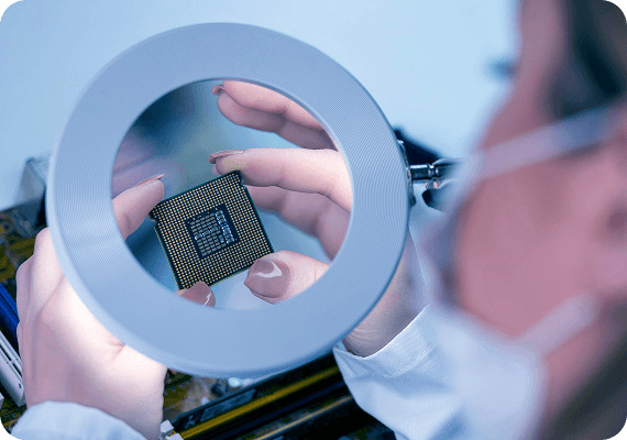
Physical Design is a crucial stage in the VLSI chip design flow where the logical circuit design is transformed into a manufacturable silicon layout. It focuses on achieving timing, power, area, and performance goals for modern semiconductor chips.
From floorplanning and placement to CTS, routing, timing closure, and signoff, Physical Design engineers play a key role in building high-performance chips used in AI, automotive, networking, mobile & advanced computing applications.
Core Backend Domain in VLSI Industry
No Coding Knowledge required
Average salary range for entry level PD Engineers in India
Global semiconductor companies hiring VLSI engineers
Six compelling reasons why this is the best investment you'll make in your career.
Build your VLSI career with confidence. Learn from ChipEdge, a leader in Physical Design training. Backed by 13+ years of expertise, industry relevance, and placement success.
Explore a career path with worldwide demand. Physical Design professionals are highly valued by leading semiconductor companies and enjoy excellent earning potential.
Gain hands-on experience with industry standard tools like Synopsys Design Compiler, ICC2, PrimeTime, StarRC, and IC Validator — widely used in top semiconductor companies for ASIC and SoC implementation.
Work on practical industry-style projects where you take a synthesized netlist and perform complete chip implementation while analyzing timing, congestion, and power.
Get resume-building assistance, mock interview preparation, aptitude guidance, and placement support through hiring partnerships and industry connections.
Build expertise that opens opportunities in advanced domains such as Low-Power Design, High-Speed Implementation, Advanced Node Technologies, and SoC Physical Design.
Choose the format that fits your schedule and learning style.
Best for freshers & students who prefer classroom-based training with direct trainer interaction.
Includes:
Best for working professionals and learners (freshers, students) who prefer online learning without relocating.
Includes:
Best for learners who want flexibility and structured content for their learning at their own pace.
Includes:
Choose the batch that works best for your schedule. Limited seats available.
Industry Standard Synopsys tools you'll master and add to your professional portfolio.
RTL Simulation & Verification
Formal Verification
Logic Synthesis
Static Timing Analysis (STA)
Physical Design & Place-and-Route
Parasitic Extraction
Physical Verification
This course is designed for anyone ready to break into tech or level up their career.
B.Tech / M.Tech Students who is pursuing pre-final/final year and want to pursue a VLSI Career in physical design.
B.E / B.Tech / M.E / M.Tech graduates from ECE, EEE, Telecom, CSE, and related branches looking to start a career in VLSI.
Professionals aiming to transition into VLSI Physical Design or upgrade their skills with hands-on industry-oriented training.
Get enrolled in 4 easy steps — the whole process takes less than 30 minutes.
Complete our quick online form with your basic details and preferred learning mode.
Our Learning Advisor will call within 30 minutes to discuss your goals and recommend the best batch.
Pay the registration fee online. Choose from full payment, installments, or education loan options.
Get access to LMS, join your batch's community, and begin your journey on day one!
Industry focused VLSI Training Programs designed to transform fresh graduates into semiconductor professionals.
Courses designed by industry experts with 25+ yrs of industry experience.
Dedicated placement support by arranging interview opportunities with leading VLSI Companies
Access cloud-based VLSI lab infrastructure and practice Physical Design anytime from anywhere.
Gain hands-on experience with industry-standard EDA tools including ICC2, PrimeTime, StarRC, and Design Compiler.
Prepare for real VLSI interviews with technical mock sessions, HR rounds, and resume-building guidance.
ChipEdge offers flexible payment options to help learners begin their VLSI journey without financial pressure.
Affordable monthly installments to spread your investment over time
No additional fees on selected payment plans
No Cost EMI as per eligibility
Take the first step towards a high-paying tech career. Our learning advisors will guide you through every step.

Talk to our expert & choose the right course for you
🔒 No spam. 100% Free. Our expert will call within 24 hrs.
Our Placement Desk works closely with leading VLSI companies to support their hiring needs for entry-level skilled engineers. We arrange interview opportunities with both multinational semiconductor companies and service-based organizations.
Placement support is provided as a complimentary service until the candidate secures a job opportunity. Registered candidates receive dedicated guidance including resume Preparation, interview scheduling, mock interviews, and career mentoring.
Hiring Companies
Learners Trained Across VLSI Domains
Group Mock Interviews, Resume Building & Interview Preparation
Placement Support Until You Get Placed


The Physical Design Training prepares learners for high-demand roles in the semiconductor and VLSI industry, aligned with current industry workflows and hiring expectations.
Through hands-on exposure to synthesis, STA, physical verification, and complete implementation flows, you gain practical skills needed for real-world ASIC and SoC design projects.
Real stories from real people who transformed their careers with ChipEdge.

I had completed my BE and I was looking for a career change. Since I had no idea about this field, whatever concepts I was learning here were new to me. Trainer support here was very good as he had a great patience and was always ready to explain concepts repeatedly till we got that.

I have done a Physical design course from ChipEdge. It is the best platform for anyone to start their career in the VLSI domain. The trainer's interact with each learner in a very friendly way. We also had industry level expert sessions every week which helped us to gain knowledge at industry level.

I have joined a physical design course in 2020. I have to say teaching is good and lab access via VPN is available. They provided a seamless experience all the way through coaching. Good experience with ChipEdge.
Everything you need to know before enrolling.
Physical Design is the backend stage of chip design where a synthesized netlist is converted into a manufacturable layout. The process includes floorplanning, placement, CTS, routing, and signoff verification. Our VLSI Physical Design Course provides hands-on training in these stages using industry-standard tools and industry-relevant projects.
Yes. With increasing demand for semiconductor professionals, Physical Design is a strong career choice in 2026. A Physical Design Certification course can help build the skills needed for backend VLSI roles in leading chip design companies.
Freshers with Physical Design Training typically earn between ₹4–16 LPA, while experienced engineers can earn as per their experience. Practical training and project experience can improve both job opportunities and salary potential.
A basic understanding of digital electronics, CMOS concepts, and logic design is sufficient to start. Most Physical Design Courses for Freshers or ECE graduates, begin with the fundamentals before moving to advanced topics.
Popular Physical Design tools include Synopsys Fusion Compiler, ICC2, StarRC, IC Validator, PrimeTime, Red Hawk & Cadence tools include Innovus, Tempus, Quantus, Voltus. A Physical Design Course using Synopsys Tools helps learners gain hands-on experience with industry-standard implementation and timing analysis flows.
Our Physical Design Training program is for a duration of 6 months. A structured Physical Design Certification program combines theory, tool training, and projects to help learners become industry-ready.
Yes. Our Physical Design Course for ECE Students is designed for freshers with little or no VLSI background.
Coding is not mandatory, but basic TCL, Perl, or Python scripting can be useful. Most Physical Design Classes introduce scripting concepts while focusing primarily on EDA tools, timing closure, and backend design flows.
Frontend VLSI focuses on RTL design, simulation, and verification, while Backend VLSI focuses on implementation activities such as floorplanning, placement, CTS, and routing. A VLSI Backend Design Course specializes in these physical implementation stages.
ASIC Design covers the complete chip development process from specification to fabrication. Physical Design is one important stage within that flow, focused on creating a manufacturable layout. An ASIC Physical Design Course provides specialized training in this backend implementation process.
Get the latest VLSI news, updates, technical resources
© ChipEdge. All Rights Reserved.


