Transition from RTL to Layout
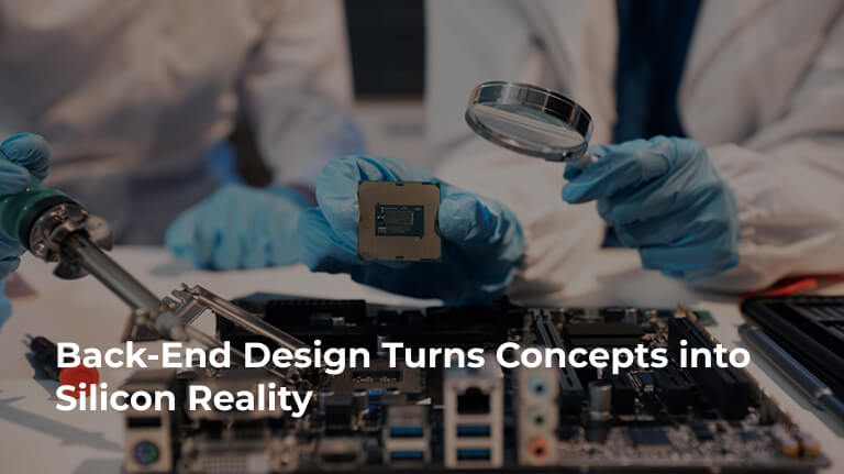
Back-end design is where things finally get real. Up until RTL, everything is just logic on paper or in code. You know what the design should do, but it doesn’t exist physically yet. In back-end, that same design gets turned into something that can actually be manufactured. You go from a netlist to actual shapes on silicon. This includes synthesis, floorplanning, placement, routing, and sign-off. Each step adds more physical detail. The tricky part is that everything starts interacting. Wires introduce delay. Power isn’t uniform. Heat builds up in certain areas. So it’s not just about connecting logic anymore, it’s about making sure it still works under real physical conditions.
Floorplanning Strategies
Floorplanning is basically your starting point for the physical layout. You decide where the big blocks go, like memories and IPs, and how the chip is shaped. These decisions matter more than they seem. If macros are placed badly, routing becomes messy later. Congestion builds up. Timing gets harder to fix. You also plan power distribution and IO locations here. Most engineers leave some extra space instead of packing everything tightly, because the design will need room later for buffers and routing. There’s no single “perfect” floorplan. You adjust it based on the design and keep refining it as you go.
Placement Optimization
Placement is where all the standard cells get arranged. Tools do most of the placement, but they don’t magically get everything right. You guide them using constraints and keep checking reports. The goal is simple in theory. Keep related logic close, avoid crowding, and reduce wire length. In reality, it takes a few iterations. You fix one issue and something else pops up. Congestion, timing, density, they all affect each other. So placement becomes a back and forth process until things start looking stable.
Routing Network Design
Routing connects cells. Metal layers. Vias.
Signal Integrity
Signals interfere. Crosstalk. Noise. Glitches. Shield sensitive nets. Route orthogonal. Space aggressors. Use differential pairs. Match lengths. Phase. Check SI rules. Coupling capacitance. Delay variation. Ensure clean signals. Reliability.
Routing Paths
Routing is just connecting everything, but it’s not as simple as it sounds. You have multiple metal layers, and you need to use them smartly. Some layers are better for long wires, some for short connections. The tools handle routing, but they still follow rules you set. You also need to watch delays, via usage, and congestion. Sometimes the tool finds a path, but it’s not the best one, so you go back and tweak things.
Timing Closure Techniques
Timing closure is where most of the effort goes. You check if signals are arriving on time, and usually, something is off. You fix it by resizing cells, adding buffers, or improving placement. Then you check again. Sometimes fixing one path breaks another, so you go through a few rounds of this. There’s no strict order like “fix setup then hold and you’re done.” It’s more iterative than that. ECO changes help here because you can fix small things without rerunning everything. Over time, you narrow down the violations until timing looks acceptable.
Power Planning Methods
Power planning is about making sure the whole chip gets stable voltage. You build a network of power lines across the design. If parts of the chip don’t get enough voltage, they slow down or fail. If current is too high in some wires, reliability becomes an issue. You don’t just rely on fixed numbers here. It depends on the design and technology. When analysis shows weak spots, you go back and strengthen those areas. It’s a bit of trial and adjustment until the power network looks solid.
Managing Physical Constraints
Constraints are what guide the tools. Without them, the tools don’t really know what to optimize for. You define clocks, delays, and exceptions so the design is interpreted correctly. These constraints need to be consistent across stages, otherwise you’ll see mismatches later. Most teams spend a good amount of time reviewing constraints because small mistakes here can lead to bigger issues down the line.
Improving Layout Accuracy
Once routing is done, you look at how the design behaves with real interconnect effects. Resistance and capacitance from wires can change timing quite a bit, so they are included in analysis. Inductance is usually only a concern in specific high-speed cases. Then you run physical checks like DRC and LVS to make sure the layout follows manufacturing rules and matches the original design. Clean results here mean you’re close to sign-off.
Handling Large Chip Designs
Large designs are handled in parts. Instead of doing everything at once, you break the design into blocks, work on them separately, and then bring them together. This makes things easier to manage. You also rely on automation and parallel runs because the data size is huge. Without a structured flow, it becomes very difficult to keep track of everything.
Ensuring Final Design Quality
At the end, you run all the checks together. Timing, power, DRC, LVS, signal integrity. The goal is to make sure the design is in a good state for manufacturing. End of physical design. It doesn’t mean everything is perfect, but it should meet all requirements with some margin. This step is more about confidence than perfection.
Delivering Production-Ready Chips
Finally, the design is converted into a GDSII file and sent to the foundry. After fabrication, the chip is tested and validated. Ideally, things work in the first version, but in real projects, small fixes can still happen. The effort you put into back-end design is what reduces those surprises. At this point, you’ve taken something that started as logic and turned it into a real, working chip.


