The semiconductor industry is defined by precision, cutting-edge technology, and highly specialized tools. While university curricula provide the theoretical foundation for VLSI (Very Large Scale Integration), the gap between academic knowledge and industry readiness is massive. Companies hiring VLSI engineers—for roles in RTL Design, Verification, or Physical Design—don’t look for candidates who know the concepts; they look for engineers who can use the tools to solve complex problems on live designs.
This critical difference is bridged only by high-fidelity lab facilities and hands-on practice. An institute that offers a robust, tool-centric learning environment is not a luxury; it is a necessity for launching a successful career in the core VLSI domain.
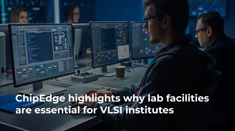
At ChipEdge, we recognize that practical exposure is the cornerstone of VLSI expertise. Our coaching programs are built around providing professionals and graduates with access to industry-standard lab facilities, ensuring you are not just certified, but truly tool-ready for the demands of a semiconductor career.
The Three Pillars of a World-Class VLSI Lab
A superior VLSI lab environment must replicate the conditions and challenges of a professional design house. This is achieved through three non-negotiable pillars:
1. Access to Industry-Standard EDA Tools
VLSI design and verification are entirely dependent on Electronic Design Automation (EDA) tools from market leaders like Synopsys. These tool licenses are prohibitively expensive and typically unavailable outside of corporate environments.
- The Challenge: Without direct practice, an engineer cannot execute fundamental tasks like running UVM simulations, performing Static Timing Analysis (STA), or executing a Place & Route (PnR) flow.
- The ChipEdge Solution: Our lab facilities provide authenticated, dedicated, and flexible access to the latest versions of these essential tools (e.g., Synopsys VCS, Synopsys Design Compiler, Synopsys ICC and Synopsys PrimeTime). This eliminates the biggest barrier to entry and ensures your learning directly translates into a valuable skill set recognized by every hiring manager.
2. Real-World Project Environment
The lab is where theory is stress-tested. It’s where you move past academic examples to grapple with the complex, multi-million gate design challenges faced by chip developers.
- Hands-on Focus: Every module in the ChipEdge curriculum is followed by intensive lab sessions. You don’t just watch a lecture on Clock Tree Synthesis (CTS); you run the CTS step on a real design block, analyze the skew and insertion delay reports, and fix timing violations.
- The Portfolio Advantage: The final capstone project, executed entirely in our lab environment, serves as a powerful, verifiable portfolio item—proving you have the practical experience required for core VLSI roles.
3. Flexible and Accessible Infrastructure
VLSI training is intensive. For working professionals transitioning into the field or students managing academic schedules, access cannot be limited to fixed hours.
- Remote Access: ChipEdge utilizes high-end, cloud-based servers and secure VPN access to provide online VLSI lab access. This flexibility allows learners to practice complex flows, debug their projects, and run lengthy simulations anytime, from anywhere—crucial for balancing professional life with rigorous training.
The ROI: Lab Skills = Placement Success
For every semiconductor company, the cost and time involved in training a new hire on EDA tools is significant. By graduating from an institute with robust lab facilities, you immediately become a priority hire.
| Skill Level | Training Focus | Job Readiness |
| Theoretical | Textbooks, Concepts (College) | Requires significant 6-12 month corporate training. |
| Lab-Enabled | Tool Proficiency, Project Execution (ChipEdge) | Job Ready from day one; minimal onboarding required. |
Hands-on training in our lab environment directly enhances your employability by allowing you to confidently discuss:
- Debugging complex functional errors in a UVM testbench environment.
- Full ASIC Flow with Signoff
- DFT Methodologies
At ChipEdge, our commitment to providing a world-class VLSI institute with lab facilities is the core of our success. It is the practical experience gained in our labs that transforms engineers from hopeful applicants into high-value, deployable VLSI professionals.
Are you ready to stop reading about VLSI and start designing? Explore the VLSI courses and dedicated lab facilities at ChipEdge and secure your future in silicon.


