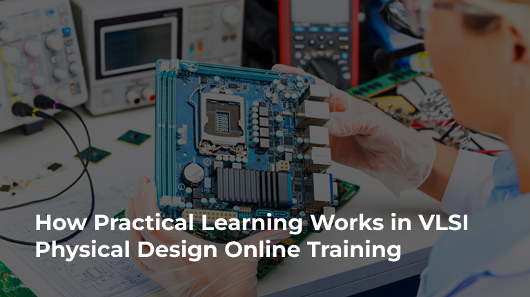
In the high-stakes semiconductor industry, a certificate is only as good as the design skills behind it. For those looking to enter the world of chip implementation, VLSI Physical Design Online Training has become the primary bridge between academic theory and industry reality.
Physical Design (PD) is an inherently hands-on craft. It is the art of fitting billions of transistors onto a sliver of silicon while ensuring they communicate at lightning speeds without melting the chip. Because of this complexity, online training has evolved beyond simple video lectures into a robust, lab-centric environment. This guide explores the mechanics of Practical PD Learning and how it transforms beginners into “design-ready” engineers.
How Online Training Builds Physical Design Skills
The most significant challenge for any fresher is the sheer scale of modern chips. You aren’t just placing components; you are managing electromagnetic interference, heat dissipation, and signal timing at the nanometer scale. Online PD training addresses this through a methodology of “Incremental Exposure.”
1. From Concept to Practice
Unlike a classroom where you might wait weeks for a lab session, PD Online Training typically follows a “Learn-then-Do” model. After a module on CMOS fundamentals or power planning, you are immediately moved into a virtual lab to execute that specific task. This tight loop ensures that abstract concepts like “leakage power” or “parasitic capacitance” become practical realities you can see on a screen.
2. Developing “Optimization Intuition”
A major part of skill-building is learning how to make trade-offs. In the real world, you cannot have the fastest speed, the smallest area, and the lowest power all at once. Online training teaches you the “PPA Triad” (Power, Performance, Area). You learn how to resize cells or add buffers to fix a timing path—developing the problem-solving mindset that recruiters prioritize over rote memorization.
Hands-On Practice in Online Training
The heart of any Hands-On Online Training program lies in its laboratory access. Modern VLSI institutes now provide cloud-based access to the same EDA (Electronic Design Automation) tools used by professionals at Intel, NVIDIA, and Qualcomm.
Industry-Standard Assignments
Learners don’t start with entire CPUs. You begin with manageable assignments, such as:
- Floorplanning a small ALU: Learning how to place blocks to minimize wire congestion.
- Analyzing Static Timing (STA): Identifying “Setup” and “Hold” violations and using scripts to fix them.
- Clock Tree Synthesis (CTS): Building a distribution network that ensures every part of the chip “beats” in perfect synchronization.
Mini-Projects: The Portfolio Builder
The transition from a student to an engineer happens during Mini Projects. These are integrated tasks where you take a small functional block (like a UART or FIFO) through the entire backend flow—from netlist to GDSII (the final layout format). These projects serve as a tangible “Readiness Indicator” for your future employers.
Learning Flow: From Basics to Implementation
To avoid overwhelming freshers, the Basics to Implementation journey is strictly modular. The sequence is vital because a mistake in the early stages of chip design often becomes impossible to fix later on.
- Foundational Phase: Mastering digital logic, Unix/Linux commands (the OS of the semiconductor world), and scripting languages like TCL or Python.
- Module-Level Mastery: Learning the individual “Big Five” of PD: Floorplanning, Placement, CTS, Routing, and Sign-Off.
- Integrated Implementation: Running a full flow where you see how a decision in floorplanning impacts the final routing congestion.
- Physical Verification: Learning how to run DRC (Design Rule Check) and LVS (Layout vs. Schematic) to ensure the chip can actually be manufactured.
Managing Consistency and Practice Online
One of the biggest hurdles of online learning is “learning fatigue.” Online Practice Management strategies are crucial for long-term retention:
- Revision Cycles: Physical design involves hundreds of tool commands. Top-tier training includes regular “Refresh” sessions to ensure you don’t forget the nuances of floorplanning while you are focused on routing.
- Time Management: VLSI tools can take hours to run a complex simulation. Successful learners treat their online training like a 9-to-5 job, dedicating specific blocks of time for tool-intensive tasks.
- Guided Exercises: Even in a remote setting, 24/7 mentor support ensures that if you get stuck on a “Routing Congestion” error at 11 PM, you have a community or a mentor to help you debug the issue.
Skill Tracking in PD: How to Measure Your Readiness
How do you know when you are ready for a professional role? Online training uses several Skill Tracking in PD metrics:
- Milestone Checks: Each module usually ends with a quiz and a practical lab test. If you can’t fix a setup violation in the lab, you aren’t ready for the next module.
- Report Interpretation: A major indicator of readiness is your ability to read a timing or power report and “diagnose” the chip’s health without help.
- Mock Interviews: Technical interviews in VLSI are notoriously difficult. Part of your progress tracking involves “Mock” sessions where industry experts grill you on your design choices during your mini-projects.
Frequently Asked Questions (FAQs)
How does online training build PD skills?
It uses incremental exposure and project-based learning to move you from basic digital logic to complex physical verification using industry-standard tools.
What hands-on practices are included in PD training?
Learners perform floorplanning, placement, clock tree synthesis, routing, and timing closure on real-world libraries (like 14nm or 28nm) in a virtual lab.
How to progress from basics to implementation?
Follow the “Flow”: start with Digital and Unix basics, master individual PD modules, and finally complete an end-to-end “Netlist to GDSII” project.
How to manage practice and learning consistency?
Set a disciplined schedule, use revision cycles to keep old concepts fresh, and leverage 24/7 tool access to practice during your peak focus hours.
How to track progress during PD training?
Track your mastery through module assessments, the complexity of the mini-projects you can solve independently, and your success in mock technical interviews.
Why is guided practice important?
VLSI tools are incredibly complex. Guided practice ensures you don’t just learn the “buttons” but understand the “algorithms” and “engineering reasons” behind every design choice.
When should learners attempt complete PD stages?
Once you have mastered individual modules and can troubleshoot timing and congestion reports on small designs, you are ready to attempt a full integrated flow.


