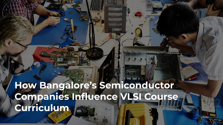
Bangalore, widely celebrated as the “Silicon Valley of India,” has evolved into the central nervous system for global semiconductor innovation. As of 2026, the city is not just a hub for design services but a critical R&D epicenter for giants like Intel, NVIDIA, Qualcomm, and Samsung. This dense concentration of industry leaders has created a “reverse-influence” model, where the hiring needs of these corporate giants directly dictate the syllabus and structure of any best VLSI training institute in Bangalore.
For an aspiring engineer, understanding this relationship is key to choosing a path that leads to a high-impact career. The curriculum isn’t just about textbooks anymore; it is about “tape-out readiness.”
The “Zero Bench Time” Mandate
In the competitive landscape of 2026, semiconductor companies in Bangalore have moved away from long, internal training programs. They expect new hires to be “production-ready.” This pressure has forced training institutes to pivot from general theory to Industry-Standard Design Flows.
- EDA Tool Proliferation: Companies like Cadence, Synopsys, and Siemens (Mentor Graphics) have their regional headquarters in Bangalore. Consequently, local institutes now provide hands-on access to the same multi-million-dollar tool suites (like Innovus, VCS, and Calibre) used in professional labs.
- Methodology Over Syntax: While university courses might focus on the syntax of Verilog, Bangalore-based institutes emphasize UVM (Universal Verification Methodology). Because 70% of the chip design cycle is now spent on verification, being “UVM-fluent” is a non-negotiable requirement set by Bangalore’s top employers.
Shift Toward Sub-2nm Design Challenges
As Bangalore’s R&D centers lead the charge into 2nm and sub-2nm process nodes, the “design rules” have become incredibly complex. A best VLSI training institute in Bangalore must now include advanced physical design constraints that weren’t relevant five years ago.
- FinFET and GAA (Gate-All-Around) Training: Standard planar transistors are a thing of the past. Modern curricula now focus on 3D transistor architectures, teaching students how to manage the heat and “leakage” issues that come with stacking transistors at the atomic level.
- STA at Advanced Nodes: Static Timing Analysis (STA) has become a massive part of the curriculum. Industry feedback has forced institutes to teach “Multi-Corner Multi-Mode” (MCMM) analysis, where students learn to ensure a chip works at extreme temperatures and voltage fluctuations.
The “Chiplet” and Heterogeneous Integration Revolution
One of the biggest shifts in 2026 is the move from monolithic SoCs (System-on-Chips) to Chiplets. Companies like AMD and Intel in Bangalore are pioneering modular designs where different “slices” of a chip are made on different process nodes.
- Interconnect Expertise: Institutes have updated their syllabus to include high-speed interconnect protocols like UCIe (Universal Chiplet Interconnect Express).
- 3D Packaging (Advanced Packaging): Because heat is a major issue in stacked chips, institutes now offer modules on Thermal Modeling and Power Integrity, skills that were once reserved for senior architects but are now expected of junior designers.
AI-Driven EDA and Automation
The semiconductor industry in Bangalore is increasingly using Artificial Intelligence to design chips. AI can now optimize the “Placement and Routing” of millions of transistors faster than a human.
- Python and TCL Integration: Gone are the days when a VLSI engineer could survive with just Verilog. Bangalore’s companies now demand proficiency in TCL (Tool Command Language) for tool automation and Python for parsing massive simulation logs.
- AI-Enhanced Design: Modern courses often include a module on “AI for EDA,” teaching students how to use AI assistants to predict circuit behavior or catch bugs earlier in the design cycle.
Focus on Specialized Verticals: Automotive and AI Silicon
The demand for silicon is no longer just about smartphones. Bangalore has seen a surge in “domain-specific” silicon design for the Electric Vehicle (EV) and Data Center markets.
- Functional Safety (FuSa): For companies like Texas Instruments or NXP, a chip failure in a car can be fatal. This has led to the inclusion of ISO 26262 standards and Design for Test (DFT) in the curriculum, ensuring chips have “self-healing” or “self-testing” capabilities like BIST (Built-In Self-Test).
- AI Accelerators: With the rise of GenAI, institutes now teach the architecture of NPUs (Neural Processing Units) and specialized memory like HBM3 (High Bandwidth Memory), which are the backbone of AI chips designed in Bangalore.
The “India Semiconductor Mission” (ISM) Influence
With India’s own commercial fabs coming online in 2026, the curriculum has expanded to include Manufacturing and Yield Optimization.
- Post-Silicon Validation: In the past, Indian engineers mostly did “pre-silicon” design. Now, with local manufacturing, there is a massive push for “Post-Silicon Validation”—the process of testing the actual physical chip after it comes out of the factory.
- Local Ecosystem Synergy: Institutes now invite guest lecturers from the India Semiconductor Mission to explain the nuances of the local supply chain, preparing students for roles in India’s emerging domestic fabs.
Soft Skills and Global Collaboration
VLSI design is a “team sport” where an engineer in Bangalore might be working with a layout team in California and a fab team in Taiwan.
- Technical Documentation: Companies have urged institutes to grade students on their ability to write clear, concise Design Specifications.
- Analytical Problem Solving: Mock interviews at the best VLSI training institute in Bangalore often focus on “debugging logic.” Companies aren’t looking for people who can memorize code; they want people who can look at a failing waveform and methodically find the root cause.
Conclusion: Bridging the Talent Gap in 2026
The influence of Bangalore’s semiconductor landscape on the VLSI curriculum is a virtuous cycle. As the city’s companies tackle more advanced global projects, the training institutes are forced to upgrade their labs, hire better mentors, and teach more complex concepts.
For an aspiring engineer, this means that the best VLSI training institute in Bangalore is more than just a school—it is an entry point into a global industry. By aligning your education with these industry-driven trends, you aren’t just getting a certificate; you are gaining a passport to the most exciting technology frontier of the decade.


